NVMe
So far, all of the PCIe drives that we’ve seen used either a number of SATA or SAS drives on an expansion card, configured as a RAID array, or utilized a custom FPGA or ASIC that required bespoke drivers to function. Neither of these was a great approach, as using RAID arrays comes with the added overhead, configuration and reliability issues. And while the custom native PCIe controllers did get around the issue, drivers were only made available to a handful of operating systems, and aside from some open source ioMemory drivers that are available on Github, I don’t even know if the other drives have any support for today’s modern operating systems.
This is where NVMe comes in. The first specification was released in January 2013 and the first drives shipped in Q2 2014. On one hand, it was a standardization of the various protocols that PCIe-native drives used up until 2013 and on the other hand, a huge improvement to the aging AHCI protocol that was originally designed for spinning disks. It greatly reduced the CPU overhead that was required to communicate with the drive, lowering the number of clock cycles that were required to perform one IO operation28. This was important, as it enabled slower, then desktop class CPUs to drive more IOPS than they would have been able to using AHCI.
It is worth noting that PCIe 3.0 was full well and alive by the time the first NVMe drives arrived, so all of them were 3.0 compatible with a theoretical max. of 0.985GB/s per lane, excluding the overhead.
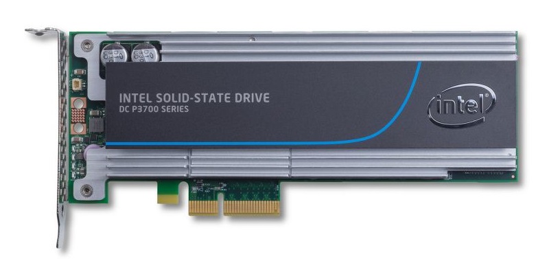
So, let’s see one of the very first drives that utilized the protocol, the Intel SSD DC P3700. It was released with its lower-endurance siblings, the P3600 and P3500. The trio was rated at 10, 3 and 0.3DWPD (drive writes per day) and the drives were priced accordingly, around $1200, $800 and $600 respectively for the smallest available 400GB capacity29.
The P3700 in Q2 2014 was rated for up to 2.8/1.9GB/s and 460/180K IOPS, which is really impressive, even by today’s standards. Fun fact, one of these drives could replace 4-6 Intel S3700 SATA SSDs in terms of performance, although it also consumes more power accordingly30, capping out at 25W. It is notable that a higher performance drive that enables faster writes will also use more CPU cycles, so some of the added power consumption, if measured at the system level, may come from higher CPU utilization. This 25W upper limit will be a common theme among PCIe and U.2 drives, with most m.2 drives coming in much lower, as they would usually target laptops where power efficiency is key.
But back to the drive, it used an 18-channel controller, which was partially derived from the S3700’s design. It was paired with 2.5GB of DDR3L for the higher capacity tiers and utilized a heatsink covering the entire drive for heat dissipation. The MLC NAND flash was made using a 20nm planar fabrication process. It has the usual enterprise features, including protection from block, page, or even total die failure.
There was a U.2 variant31 as well, using the SFF-8369 connector, which was essentially a 2.5″ drive that used four PCIe lanes, just like the PCIe HHHL version.
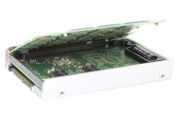
Just like most U.2 drives, this was 15mm thick, more so than a normal 2.5″ SATA drive and that’s because the controller itself required more PCB space and more thermal mass and surface area to dissipate that heat, so the bottom of the drive had some fins and acted as a heatsink. Consequently, the added NAND flash required to feed the 18-channel controller required another PCB that used a flex cable on one side to connect to the controller. There is also a fairly sizeable cap for power loss protection. This is still a common theme among enterprise U.2 drives, although there are some 7mm drives around that use lower power controllers that are popular with m.2 drives and fewer NAND packages.
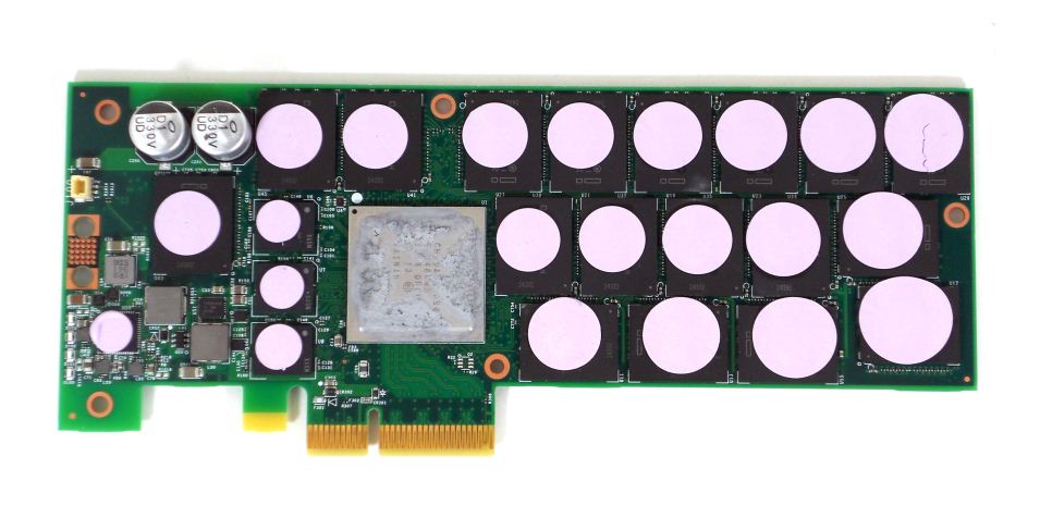
Samsung’s entry to the game was the XS171532. It was announced in the summer of 201333 and became available in Q3 2014 as a U.2 drive. Rated at 3.0/1.4GB/s and 750/115K IOPS, it was a bit different from the P3700. Faster reads and slower writes. It used a PMC 89HF16P04CG3 controller with 2GB DRAM, so this is curiously not a fully in-house drive, but I suppose it was more economical to use an off-the-shelf part instead of developing their own enterprise-grade controller. It offers ECC and flash-channel RAID, so the data is still recoverable in the event of NAND failure.
The above shows the internals with the PMC controller, three RAM packages, which I suspect support ECC and the two larger ones contain 4 dies each, while the smaller one is just a single die for the ECC. This also had a 15mm z-height, just like the P3700, but instead of flex cables, it used a pair of high density connectors on each side.
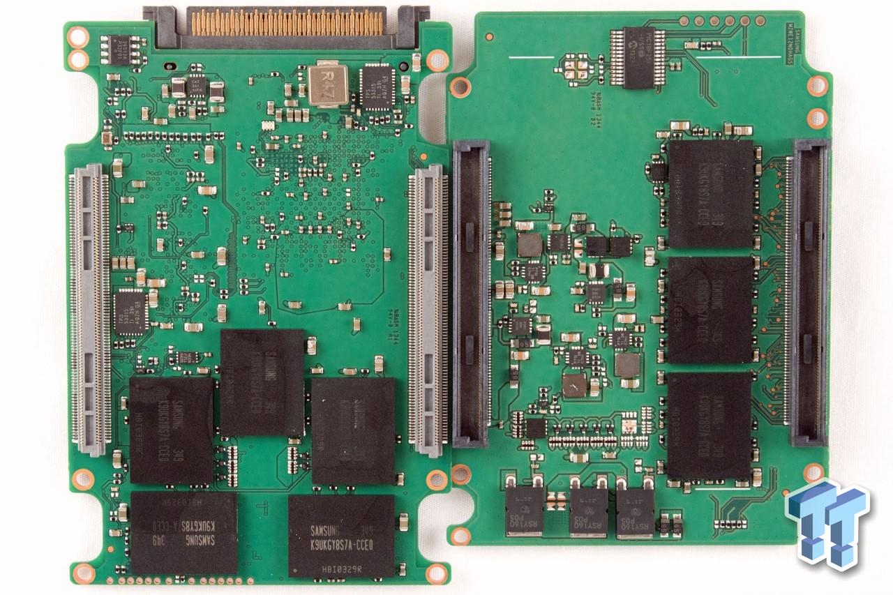
There are a total of 16 NAND packages, utilizing planar 20nm eMLC NAND. The ‘e’ stands for enterprise, so this is a high durability variant, which is rated for more r/w cycles than consumer MLC. The above shows the connectors that allow the two PCBs to communicate and on the other side of the PCB on the right, there is a bank of tantalum capacitors for PLP (power-loss protection). The SFF-8639 connector is also clearly visible at the top. It uses a layout that’s very similar to SAS drives, but has an array of added pins on the other side of the connector. This allows the use of the same physical design for SATA, SAS and U.2 drives, allowing the use of the same backplane (if it’s correctly wired) for both SATA/SAS and NVMe drives.
These drives are also dual-port capable. What that means is that they can split up the PCIe lanes and create two separate data paths to the host. While doing this doesn’t make much sense with a HHHL drive, like the one in the picture, a 2.5″ drive with the U.2 connector can benefit from this, essentially having two separate PCIe x2 connections to one or two hosts. This increases availability by creating two fault domains. A similar architecture is found in most SAS SSDs as well, where they have two SAS ports that can be wired to two separate controllers or used together to increase bandwidth.
The next generation of enterprise drives
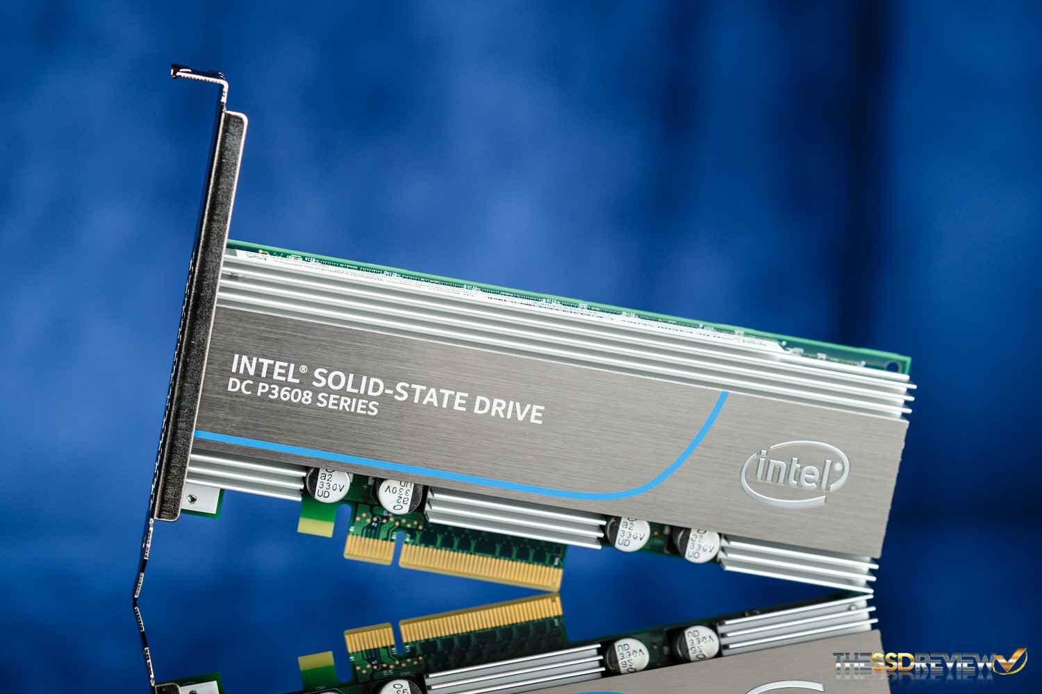
I like interesting solutions, especially for problems that didn’t really exist in the first place, so meet the Intel SSD DC P3608. Intel has seemingly refused to build a drive that natively supports an 8-lane PCIe uplink, which makes sense, as U.2 can only use up to 4 lanes and they likely don’t sell enough HHHL cards to justify the cost of developing an 8-lane controller. But they did in anyway. Sort of.
The P3608 does indeed have an 8-lane connector and all the pins are wired up the way they are supposed to. The drive, too, is rated at 5.0/3.0GB/s and 850/50k IOPS, so that’s wrong? Wait, 50K write IOPS? That doesn’t look right, but it is. Let’s see what they did here.
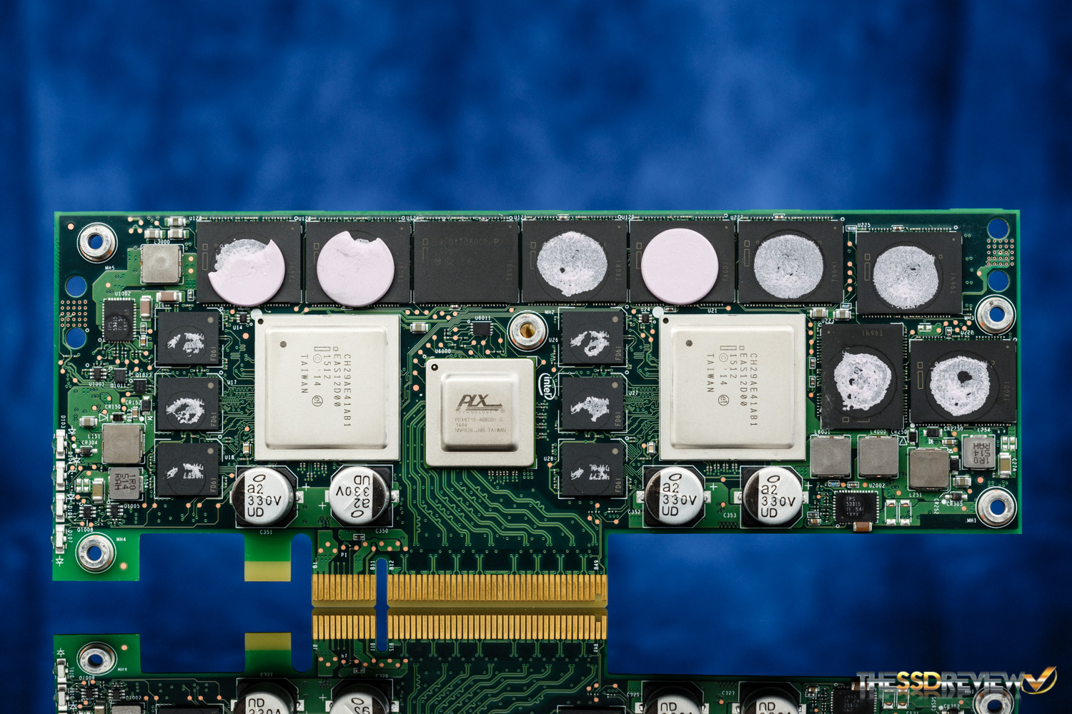
Oh yes, it’s just two DC P3600 SSDs glued together. Kind of like the SLI of SSDs. It uses the same controllers as the P3600 and has the exact same feature set, along with a PLX PEX8718 switch chip between them. It essentially shows up as two separate drives to the OS and the rated speeds are achieved when the two drives are used in RAID0. Not the cleanest solution. With the two controllers, also came a fairly high power consumption of 40W. Just for the record, it was released in Q3 2015.
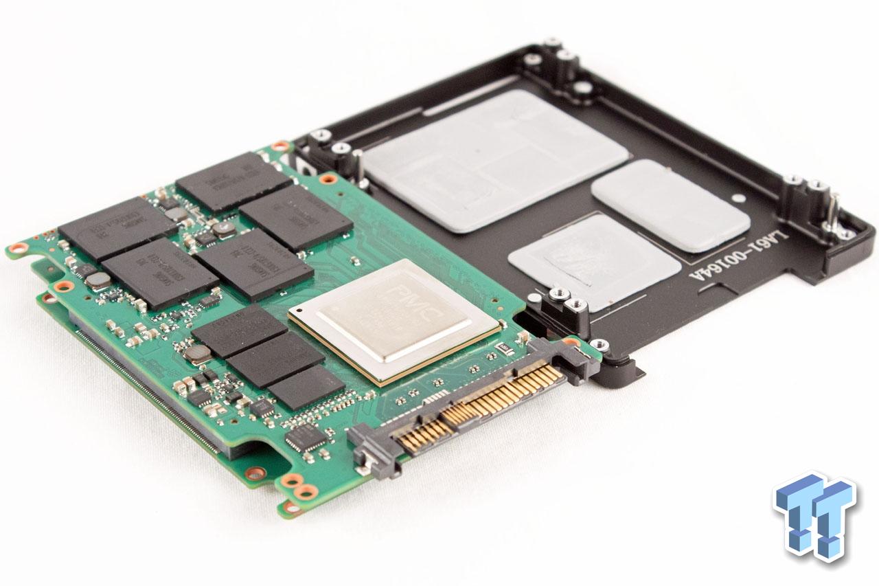
Samsung took a much better approach with the PM172534, although it came about 1.5 years later in Q1 2017, with the slightly optimized PM1725a replacing it about a year later. The drive uses Samsung’s own Epic controller, featuring 16 channels and 8GB of ECC DDR3 RAM. The NAND is also their own 48-layer 3D TLC flash35.
Rated at 6.2/2.6GB/s and 1000/180k IOPS for the PM1725a at all capacities, these are real enterprise drives, and could compete with much more recent PCIe 4.0 m.2 drives. They do need 25W to achieve these speeds, but that’s standard for this segment.
This drive also supports NVMe namespaces36, which allows the creation of virtual block devices within a single NVMe drive. This can be very useful for virtualization, when one drive needs to be split up between multiple VMs. Namespaces allow different sections of the drive to be passed through to different VMs directly as a PCIe device, without having to create VHD files and push everything through a software layer, which only adds extra overhead and complexity.
Some more eye candy
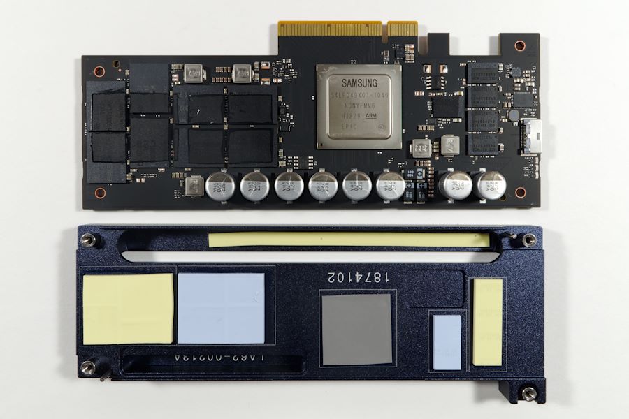
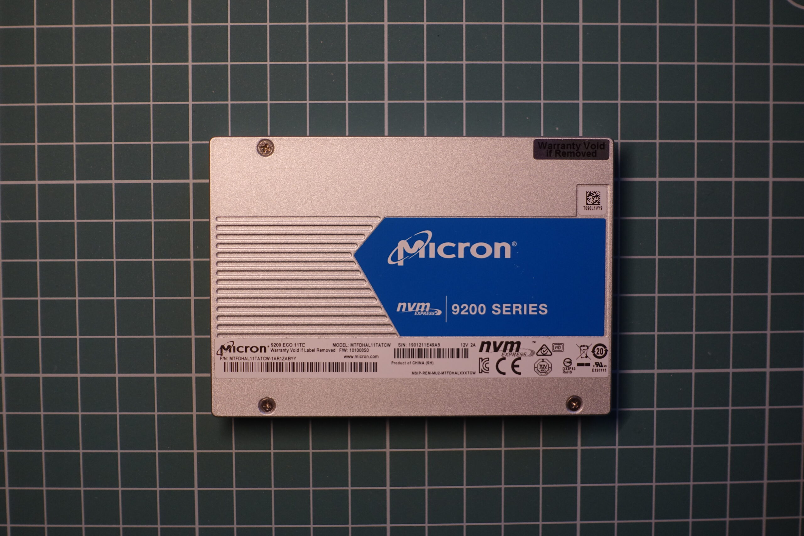
The below is an 11TB Micron 9200 Eco. Released in Q3 of 2017, these jump ahead of the timeline a bit, but since the internals of the drive are very fascinating, I wanted to include it somewhere. The drive uses 3D TLC flash and is rated at 3.5/3.5GB/s and 840/130k IOPS, which pretty much saturates a 4-lane PCIe 3.0 connection. The controller itself actually has an 8-lane interface, but the U.2 interface of this particular drive only allows the use of half the avaiable lanes.
The Micron 9200 series was also available in two other lines, the PRO and the MAX. The ECO drives were aimed at read-intensive workloads, whereas the PRO was for mixed use and MAX was for write-intensive use. They had increasingly more over-provisioning
Since this is Micron’s crème de la crème, it supports PLP, flex capacity, which is a way to manually adjust the amount of over-provisioning of a given drive, increasing endurance in lieu of some of the capacity, so one could technically turn a PRO drive into a MAX drive by increasing the size of the spare area.
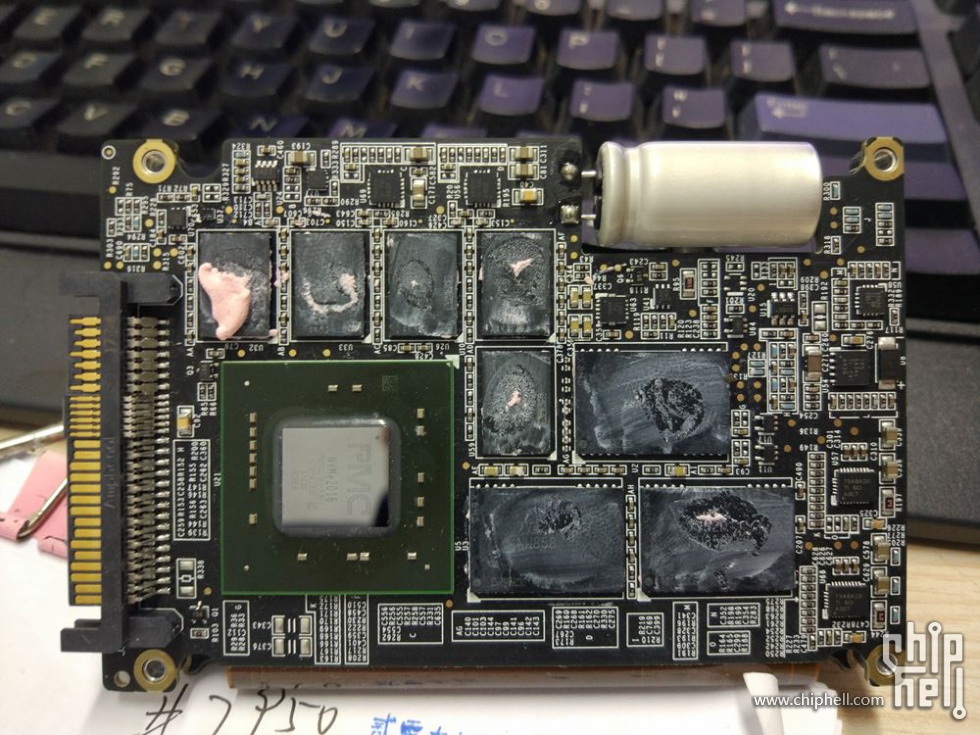
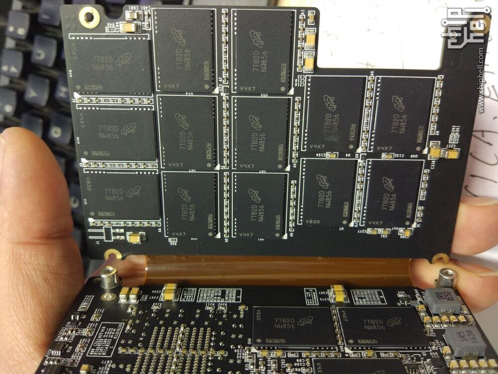
The controller is a 32-channel PM8607 NVMe2016 from Microsemi37, paired with 32 NAND packages and nine DDR3 packages with ECC support. Most of the NAND is on a daughterboard, which uses a flat ribbon cable to connect to the main PCB. This two-board design is very common in 15mm 2.5″ drives.
The drive itself uses a lot of power, which shouldn’t be a surprise. That controller is as big as a smaller GPU. A fun fact however is that the manual states that “The 9200 is not intended to be a bootable device. Boot functionality is not validated by Micron, and any use in this manner is done at the user’s own risk.” I love it. It clearly states that they can’t be arsed to support boot issues and to be fair, they really shouldn’t. If someone has the money to buy one of these, they should be able to throw in a SATA drive as well to boot from. Oh, and by the way, it does show up in the boot menu, so I’m quite certain it woudl work just fine, but who in their right mind would use an 11TB drive to boot from?
Leave a Reply