This article has taken over four months to complete and required a considerable amount of time to write, as well as to ensure correctness and all the parts are intertwined as to give the reader a pleasant and fluid reading experience. I hope you enjoy reading it as much as I enjoyed typing it up.
I’ve always found computer hardware fascinating and had an interest of how all the components came together and functioned to create an impressive product, whether it was a graphics card, network switch, motherboard or SSD.
In this article, I will attempt to expound the history of solid state drives and the technology behind them. These devices are incredibly ubiquitous nowadays, but that wasn’t always the case, as most of us had hard drives in their computers as little as 10 years ago, at least for bulk storage.
Since raw lexical facts can be found on Wikipedia, I will mainly focus on how the architecture evolved and include examples of the bleeding edge of solid state technology from each year.
SSDs date back to 1991, with the first example being a 20MB PCMCIA, expansion card, which is a hot-pluggable implementation of PCI for laptops and other portable devices. That’s way too old to be comparable to anything that’s around today, so instead, I would like to focus on more contemporary drives which can be used in a modern computer, which will put us at 2009.
But first, let’s look at what makes these drives work.
The internals of an SSD
Modern SSDs are essentially mini computers with a proper ARM-based CPU that usually has its own RAM and interfaces with the NAND flash and the host computer, using a SATA, SAS or PCIe interface or something even more exotic.
Let’s start dissecting the most important part first, the NAND flash.
Flash memory is an electronic non-volatile computer memory storage medium that can be electrically erased and reprogrammed. The two main types of flash memory, NOR flash and NAND flash, are named for the NOR and NAND logic gates. Both use the same cell design, consisting of floating gate MOSFETs. They differ at the circuit level depending on whether the state of the bit line or word lines is pulled high or low: in NAND flash, the relationship between the bit line and the word lines resembles a NAND gate; in NOR flash, it resembles a NOR gate.
Flash memory – Wikipedia
That is a very concise definiton, but it doesn’t describe it well enough. I would like to dive into the inner workings of the cells themselves a little further. The main component of a NAND cell is a floating gate (FG), which is insulated by oxide layers, preventing the electrons from leaking out of it. Any electron stored in the floating gate is trapped, which means the cell is charged and has a binary value of 0. When it holds no charge, its binary value is 1.
Several of these are connected in series to form a string and these strings are vertically arranged to form a block. A NAND page is a group of cells that belong to the same block, which share the same control gate or word line. A NAND block is composed of several pages. Several NAND blocks form a plane and planes form a die, which is a physical piece of silicon. Each memory package may contain one or more of these dies.
Read and write operations are carried out on a page, which is usually 8-16KB. To write to the flash, several high voltage pulses (10-20V depending on cell type) are applied to the control gate. During each pulse, electrons move from the iso-p-well to the floating gate, essentially increasing the threshold voltage of the cell. This operation degrades the cell and this wear out is why they are rated to a limited number of read and write cycles. Erase works the same way, but uses negative voltages. To read the data stored in the cells, the stored voltages are compared with a threshold voltage and the controller determines whether the cell stores a 1 or a 0 in the case of an SLC cell.
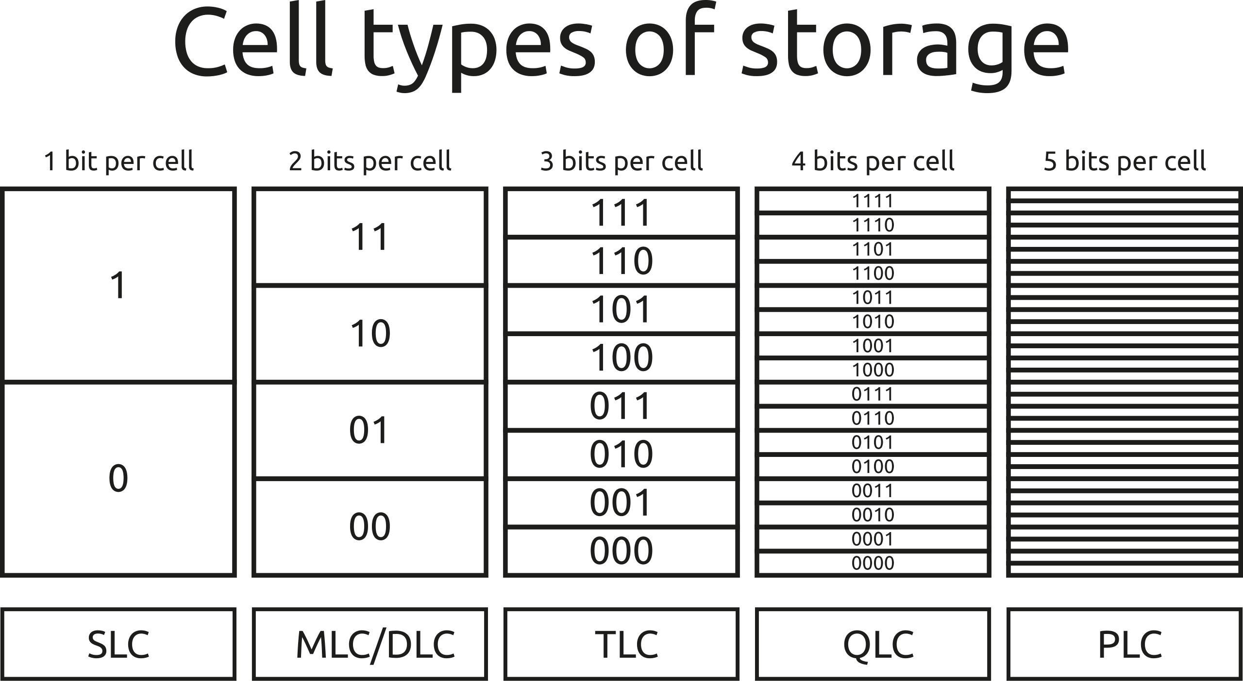
And finally, we got to the different cell types. SLC is the most basic cell type, where the cell voltage is either high or low. This is the fastest to read or write and has the highest endurance, while also being the most expensive of all cell types.
And by all cell types, I mean SLC, MLC, TLC, QLC and perhaps PLC as well, in the future. But what does all this mean? SLCs or single level cells can be either low or high and thus store one bit in a cell. Simple enough. MLCs or multi level cells are really dual level cells (they just didn’t want to call them DLCs, as that would have likely caused some confusion within the gaming industry) which store two bits in one cell. How they do it? They use not two, but four voltage levels for the four possible states of the two bits that are stored in each cell. These are [00 01 10 11]. This means that the controller needs to be able to reliably discern these voltage levels from one another. This is more difficult than it is for SLC cells, and MLC cells are also rated for fewer write cycles than the SLC counterparts. But the upside is that now we can store twice as much data per cell. This essentially halves the price of the NAND flash. TLC stores three bits per cell, which have the following permutations: [000 001 010 011 100 101 110 111]. Note that there are now 8 possible combinations, which means the controller has 8 voltage levels to deal with, and instead of doubling the capacity, we’re only increasing it by 1/2 or 50%. QLC stores four bits per cell with 16 possible permutations and voltage levels for a mere 1/3 or 33.3% increase in per-cell capacity while substantially reducing the available write cycles due to the tiny differences between the 16 voltage levels.
PLC or penta level cell drives will become a reality in the coming years thanks to more advanced controllers, but they will only gain a 25% increase in per-cell capacity, while suffering a serious hit in endurance due to the 32 distinct voltage levels that need to be reliably differentiated in the cells.
This diagram illustrates the issue very well:
The other important part is the controller itself. As I mentioned above, this is a self-contained system with its own CPU cores and RAM. It uses a standard interface to talk to the host and has a number of flash controllers, using the Open NAND Flash Interface standard to talk to the cells. There is also a lot of magic under the hood, such as ECC, TRIM and garbage collection and while those are fascinating on their own right, this article is not going to delve into them.
What I would like to talk about is performance. The performance of the NAND flash itself depends on the number of levels the cells have. SLC is faster than MLC, MLC is faster than TLC and so on. Manufacturers often operate part of the NAND with fewer levels than the rest of the drive to cache writes and then shuffle the data to the slower flash. For example, if you have a 1TB TLC drive, it might have 30-60GB that operate in MLC mode, speeding up the writes. This is called a write cache and can be really useful, unless it fills up, in which case the writes will slow down. Once the write cache is written to, the drive will slowly shuffle the data over from the MLC area to the TLC area in the background. This is fully independent of the host and does not need any software or driver support.
The other aspect is the presence of the onboard RAM. This is usually used to store the data mapping tables, which essentially describe where the data is saved on the flash cells, as well as a cache for buffering the data that’s to be written to the NAND cells to reduce write amplification. Write amplification happens when the data block that the host attempts to write on the drive is smaller than the block size of the SSD, so even when the host writes a 4KB file, the SSD needs to overwrite an entire 128KB block, because that’s the smallest allocation unit it can access in one go. Caching writes and bundling them into 128KB (or whatever the smallest allocation unit is) blocks can help speed up the write performance of a drive.
There is a technology called HMB or host memory buffer, which allows the SSD to access the system RAM for storing these mapping tables, which does help, but it isn’t as fast as a dedicated RAM chip. This is only available on newer NVMe drives, as it requires the PCIe bus to access the system memory using DMA.
And finally a controller can have a varying number of NAND flash controllers. These are somewhat analogous to memory channels on a PC. The more you have, the more cells you can talk to in parallel, although these also increase the complexity and power consumption of the drive. Most consumer drives have 8-channel controllers, while in the enterprise market it’s possible to find 12 or even 16-channel variants. What I would like to point out is that with the more modern packaging technologies, one physical NAND package (that black “chip” on the PCB) may contain multiple silicon dies inside and therefore it’s possible to feel an 8-channel controller with only two NAND packages that have 4 dies each.
Leave a Reply