V-NAND
Arguably, this did not directly affect the speed or performance of drives, but it made the NAND flash faster, more compact and more durable.
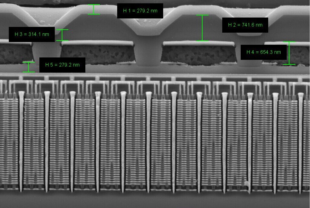
V-NAND stands for Vertical-NAND. This technology allowed Samsung to vertically stack the NAND cells on top of each other, increasing the per-die capacity and yet, creating a die with a footprint that’s smaller than conventional 2D NAND. There are many great resources explaining how this works, but to keep it simple, imagine that you have a fixed size plot, which is the die. 2D NAND would fill that up with single-story houses, crammed up next to each other as close as they can possibly go. Let’s say 10×10 buildings on the plot. With 3D NAND, they managed to replace these with 7×7 32-story towers. This not only increases the number of “apartments”, but also allows them to have a larger footprint.
This way they have 32 layers of cells in a 3D structure, stacked on top of each other, and each cell can have a larger surface area, allowing for a higher endurance, while the die itself is slightly smaller than conventional 2D NAND.
The first consumer drive to use it was the Samsung 850 Pro, putting us at Q3 of 2014. If I wanted to be quick, I could just say that it’s another chart-topper from Samsung and I wouldn’t be very far from the truth, but let’s dig in a bit more.
First off, the V-NAND that these drives used did not come in binary capacities. Traditionally, 2D NAND dies were manufactured in capacities that were powers of two. 4, 8, 16Gb per die. The 40nm MLC V-NAND that is used here has a capacity of 86Gb per die, which is quite unusual. This means that while the drives were sold in capacities of 128, 256, 512 and 1024GB (Yes, we’re finally in the 1 terabyte range) the underlying raw capacity of the NAND was 129, 258, 516 and 1032GB with 7.6% of over-provisioning18. It is also noteworthy that while planar NAND technology was using 19nm manufacturing at the time, V-NAND was manufactured at 40nm, as stated above. This is the difference that enables the higher endurance of V-NAND while the vertical stacking increases capacity.
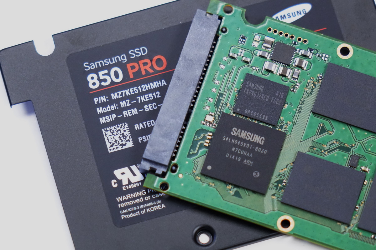
The drive uses the MEX controller from Samsung featuring three ARM Cortex R4 cores, which was previously seen in the 840 non-Pro and interestingly, they coupled it with 256/512/512/1024MB of LPDDR2 for the 128/256/512/1024GB capacity points, which is not linear. Even the smallest 128GB model boasts speeds of 550/470MB/s, which is not that far off from the 1TB model’s 550/520MB/s and 100/90K 4KB random read/write IOPS. Speaking of a terabyte, it cost $700, which was nowhere near as cheap as today’s drives, but considering that just two years ago the 512GB 840 Pro cost $600, the price-per-GB ratio was certainly better. The more popular 128/256/512GB capacities were sold at $130/$200/$400, so one could realistically afford to get a 256GB drive for the OS without breaking the bank. In fact, I had one of these back in the day and it was a great drive. Still is, although PCIe-based drives have mostly overtaken that position by now.
Leave a Reply