Bringing NVMe to the mainstream
All we’ve seen so far have been enterprise drives, because as always, that’s where the all the new tech lands first. However, they are bound to reach consumers within a short period and that’s what happened here as well.
The first high-end NVMe drive to be released specifically for workstations and custom builds was the Intel SSD 75038 in Q2 of 2015. It is very similar in appearance to the Intel P3X00 drives, which is no coincidence, as it was based on the P3700, with some firmware tweaks. Among those is the much more digestible idle power at 4W instead of constantly consuming around 15W and some optimizations of the random write performance. The peak power consumption of the 1.2TB model is still 22W, but the heatsink provides enough thermal mass to keep it cool for those occasional bursts.
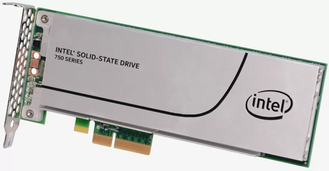
The PCB is identical, so I won’t include images of that. The drive was rated at 2.2/1.2GB/s speeds and 440/290K IOPS for the 1.2TB capacity, which doesn’t seem to be much nowadays, but it was top tier performance and it was sold for $389 and $1029 for the 400GB and 1.2TB capacities. The 1.2TB drive used 1,376GB of flash memory, which means 18.8% of the total space was used for over-provisioning, which is quite a lot for a consumer drive. But then, this was really a rebranded enterprise drive, so it’s not exactly a surprise. I wonder if they had different assembly lines for the 750, or they just used their P3700s, flashed a different firmware on them and slapped on a redesigned heatsink.
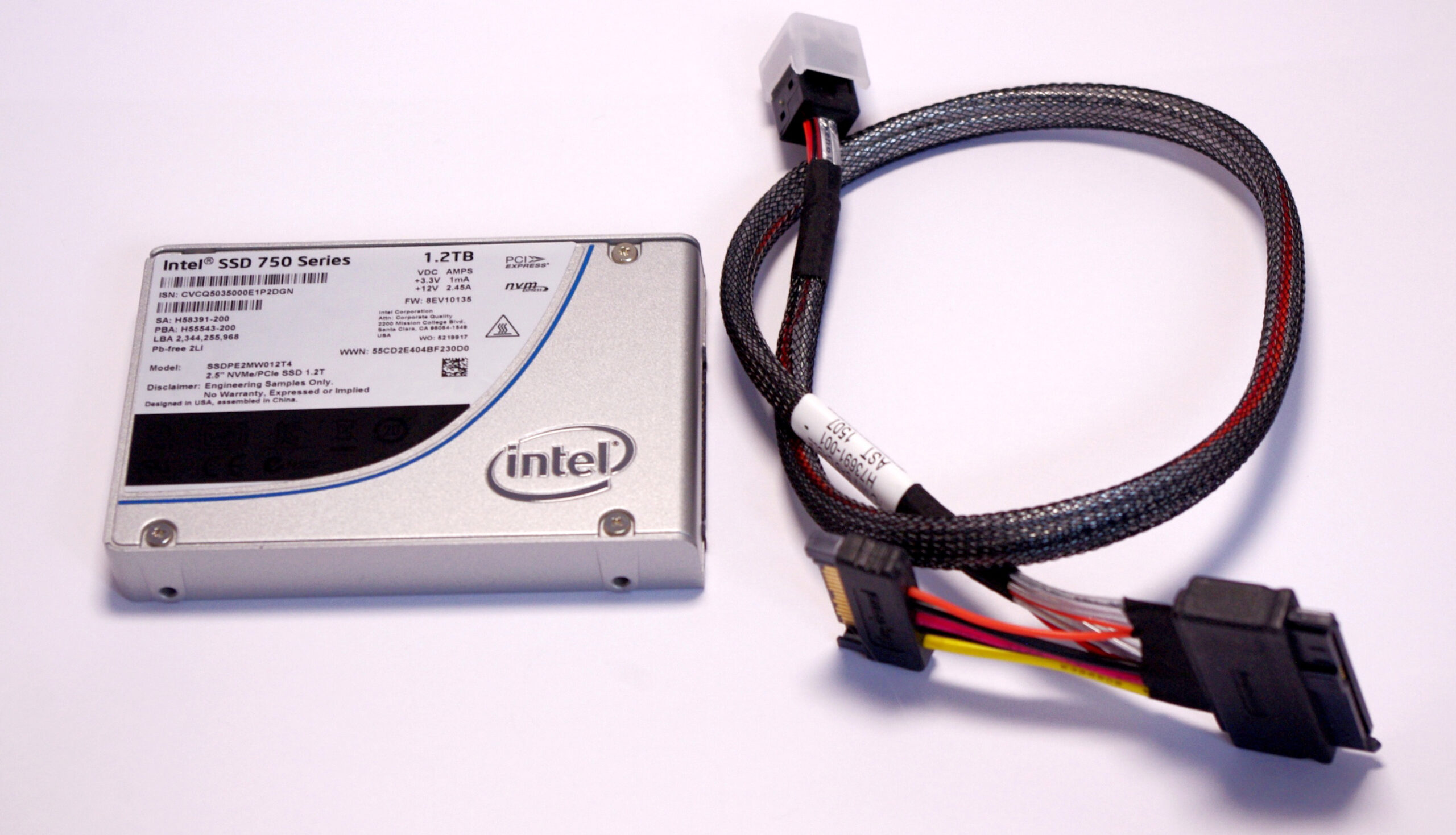
There was a U.2 as well, version with an SFF-8639 connector and identical specs. this is another 15mm thick drive, as the bottom of the enclosure also plays as a heatsink.
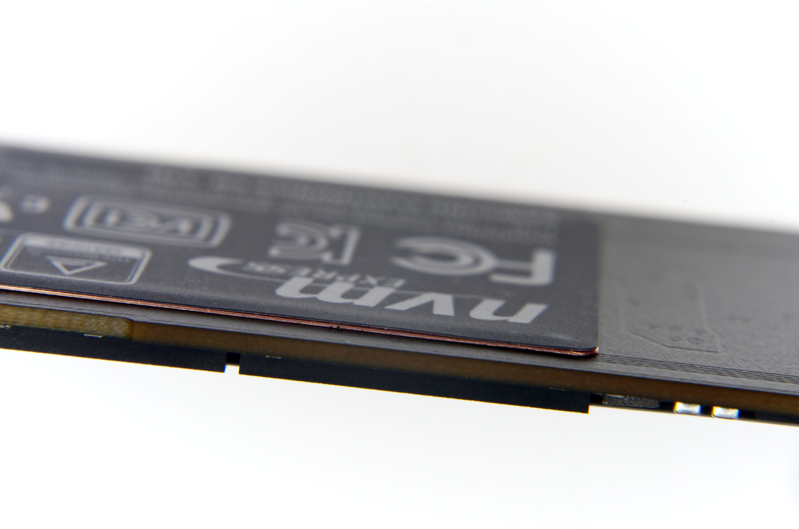
Just a few months later, in Q4 of 2015, the Samsung 950 Pro39 was released. This was very different from the Intel 750, not only because it was an m.2 drive, but it was also designed for clients from the ground up. It uses Samsung’s more modern 32-layer 3D MLC V-NAND, alongside their 8-channel, triple core UBX controller and 512MB of DRAM.
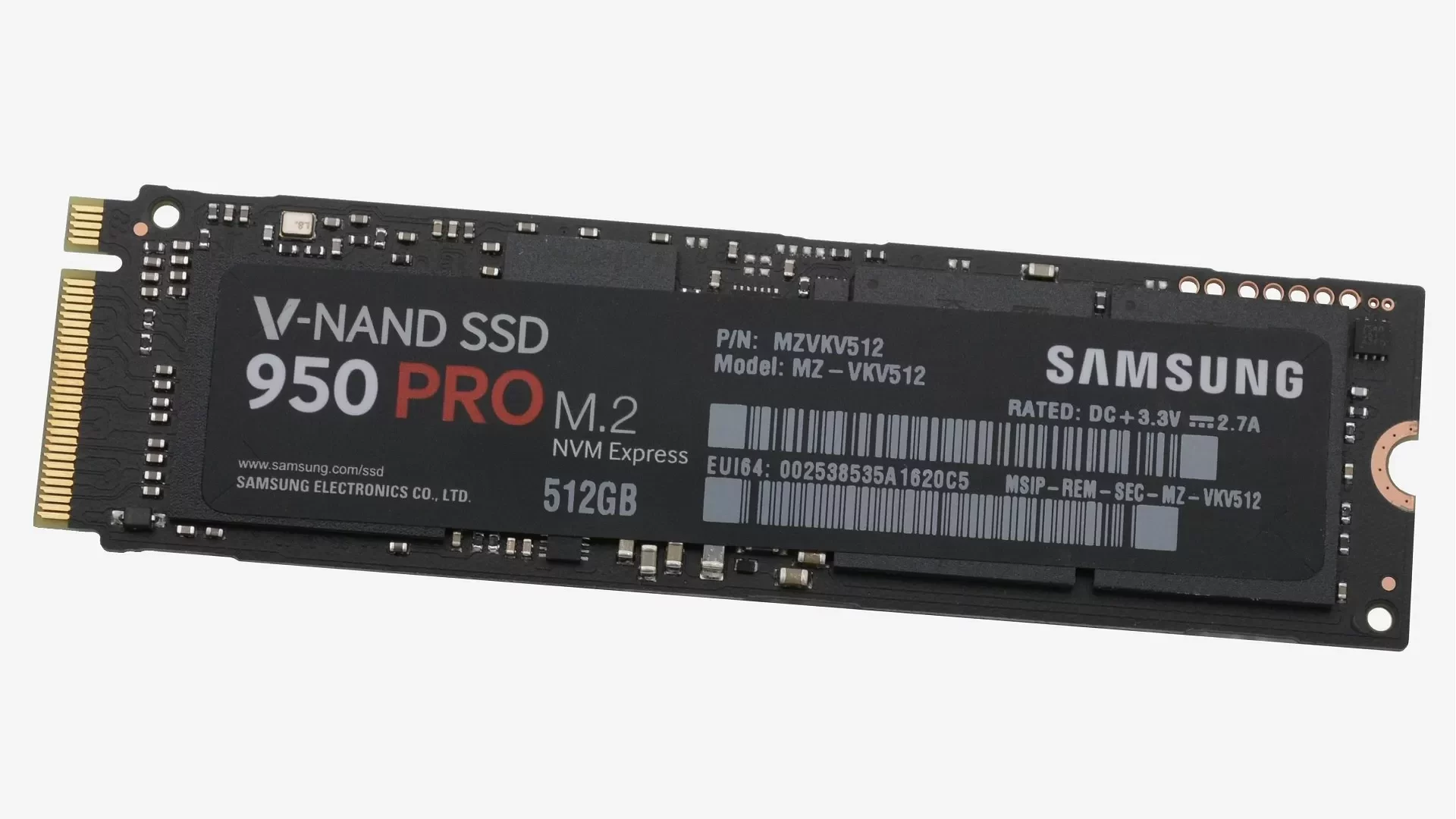
This package was enough to reach 2.5/1.5GB/s speeds and 300/110k IOPS for the 512GB drive, which is incredible if you compare it to a HHHL drive. It looks tiny and incredibly simplistic, but then, it didn’t consume much power, idled at 1.7W and only used up to 7W under load.
Samsung had another m.2 drive, the SM95140 that came out a few months earlier, but that was OEM-only, you couldn’t find it on the shelves. It had slightly lower read speeds and 16nm planar MLC NAND, but the controller and RAM size was identical.
The 960 Pro41 arrived exactly one year later in Q4 2016 and offered increased performance and capacities up to 2TB. It was even faster at 3.5/2.1GB/s and 440/360k IOPS for the 2TB capacity at just 5.8W. The controller was upgraded to the new 5-core Polaris with 8 NAND channels. The drive also features an interesting cooling solution. Silicon Motion’s SM2260 controller used a copper heat spreader on the top of the package, just like all socketed CPUs do, but Samsung decided to add a layer of copper to the drive label, stuck on the back, to spread out the heat produced by the controller alongside the length of the drive. But this is only the tip of the iceberg.
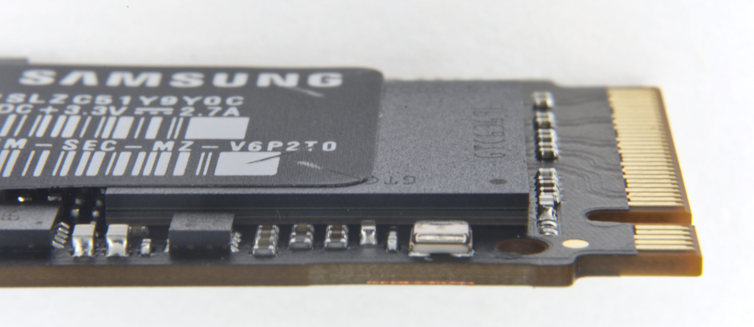
The 960 Pro used Samsung’s 48-layer 256Gb MLC V-NAND. That’s 256 gigabits or 32 gigabytes per die. To achieve 2TB with these dies, they needed 64 of them. However, on an m.2 drive, space is at a premium and seeing that they wanted to keep it single-sided, they had to put all four NAND packages on one side. One of these contained 16 dies for a capacity of 512GB. This used up most of the real estate on the front and didn’t leave much for the controller. Looking at the image below, there simply wasn’t any space left for the DRAM and this is clearly not a DRAM-less drive.
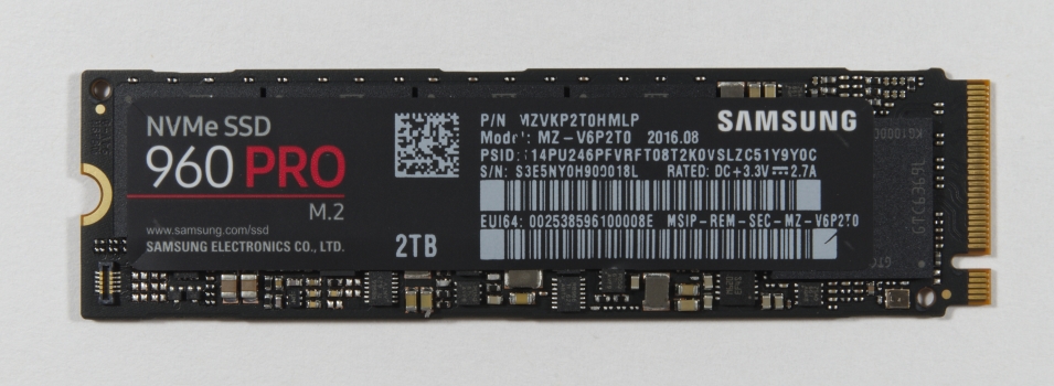
That’s because it moved on top of the controller. Since they also manufacture phones and SoCS where PoP (package-on-package) chips are very commonplace, they must have been pretty familiar with the technique already. The top layer is the DRAM with the controller underneath, interfacing with the DRAM on top using microbumps and soldered to the PCB at the bottom with a somewhat smaller footprint to save even more space, as the pins of the DRAM interface didn’t have to be added to the bottom contacts. I have not seen this construction on any other drive since the 960 Pro.
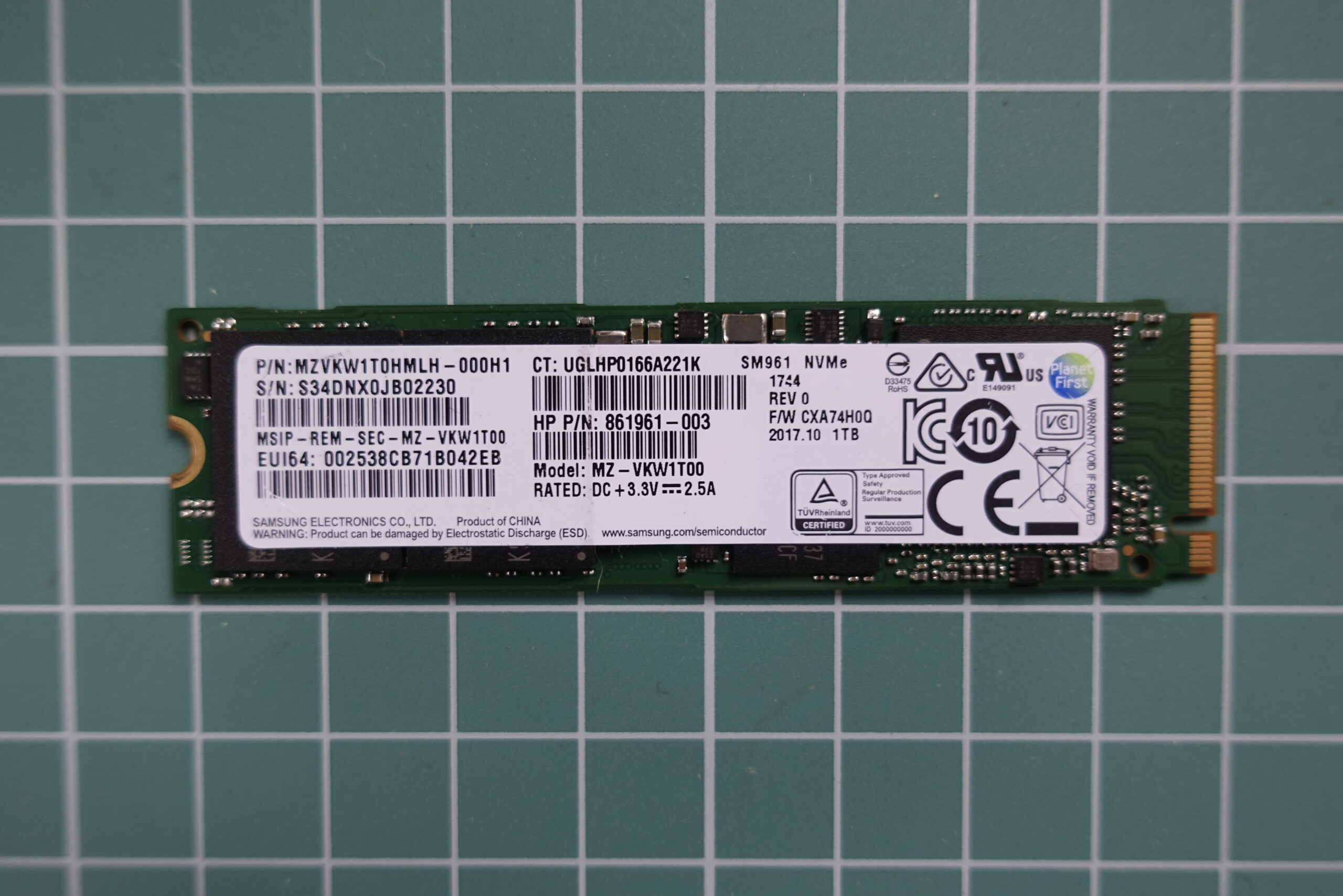
What I find really interesting is that they used the same layout for the smaller, 1TB and 512GB models, even though they could have used a more traditional controller with a separate DRAM package and two NAND packages, just like the SM961 did, which is essentially the OEM version of this drive.
Speaking of the SM961, it’s the same drive with a more traditional layout that includes a separate controller, a DRAM chip and two NAND packages on a lovely green PCB. But the architecture is exactly the same with the third-gen 48-layer 256Gb MLC V-NAND, the Polaris controller and the usual 1GB RAM for each TB of storage. And sure enough, the performance is also very much in line with that. My SM961 came in at 3.5/1.9GB/s and 440/340k IOPS, which is very close to the 960 Pro and the difference is likely due to a somewhat different firmware that may run the CPU or RAM at slightly lower clockspeeds.
The next few generations of m.2 drives were very much the same with an 8-channel controller that used four PCIe 3.0 lanes to communicate with the CPU. I don’t really want to list up all the different variants, but there are a few interesting drives that got released during this time.
m.2 2230 drives
These are (very obviously42) 22x30mm drives, or the shortest standard form factor available for the m.2 interface. We got some really interesting packaging techniques from Toshiba/Kioxia and Samsung, as well as Phison later on.
The first such drive was the Toshiba BG1 that was announced at CES 201543. Thay managed to pack an entire drive in a single 16x20mm BGA package. Sure enough, the capacity topped out at 256GB and it only had an x2 PCIe 3.0 link to the host, but it was an NVMe drive nonetheless. It was the world’s smallest NVMe drive at the time and it was aimed at replacing SATA and eMMC drives in small devices instead of being a performance champion.
The next generation, the BG2 came with HMB support, which means that the drive could store the L2P (logical to physical) mapping table in the host’s memory. There is a great deep-dive on the technology here. HMB is part of the NVMe 1.2 specification so in theory, all drives that support it should be capable of using HMB. It’s usually a small, 32-64MB portion of the RAM, nowhere near as much as a dedicated DRAM chip would be.
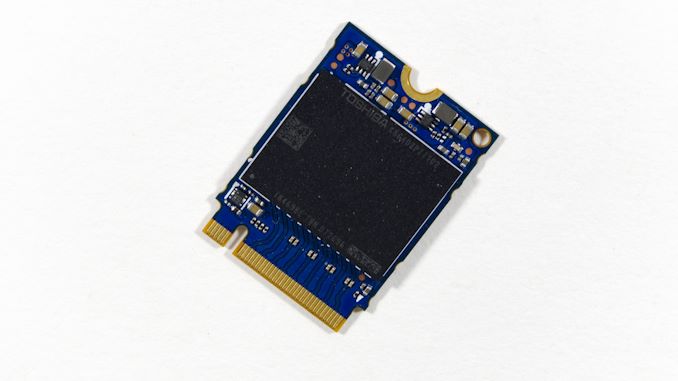
Above is a Toshiba BG4, which looks exactly the same as all other BG-series drives from Toshiba, I simply wanted an image that shows the ship without a label. This is a 4-lane drive, you can see the four differential pairs going from the chip to the edge connector with the pairs of SMD capacitors. The far edge of these drives is usually used for the power circuitry and there is not much else on these drives.
Nearly all of them are DRAM-less, with the only exception that I could find being the Samsung PM97144. It has Samsung’s dual-core Proton controller, paired with DDR4 RAM and MLC V-NAND45. Despite that, it was quite sluggish at 1,500/900MB/s and 190/150k IOPS, although in the BGA category, it was faster than anything else that was available at the time. Especially since anything else in this context means the Toshiba BG2 which was rated at 950/400MB/s46 for the 512GB model and used 3D TLC NAND47. Both of these drives used two PCIe lanes to communicate with the host.
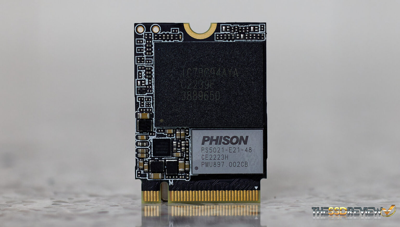
As HMB became more and more popular, these 2230 drives all started using and requiring it to deliver their advertised speeds and without it, they often perform significantly worse. But it makes sense, as not having to include DRAM chips in the same packaging, along with the controller and NAND flash simply leaves more space for the flash. Lately, the use of physically smaller, four-channel controllers have become really popular in this space, as they give more flexibility to the manufacturer with what size and type of NAND they use with the controller. The below is an example of this, although this is a much newer PCIe gen4 drive from Sabrent, but all drives of this style use a similar construction.
The Xbox Series X uses a similar drive, the WD SN530, which is rated at 2,400/1,950MB/s and 400k/400k IOPS. It uses 14nm, 96-layer TLC flash from Toshiba and there are sixteen 512Gb dies in the single flash package for the 1TB variant.
Flash speeds
Most standard m.2 drives used an 8-channel layout, especially if they were marketed as a high-performance device. Those 8 NAND channels were required to reach the advertised speeds, not always warranted by the targeted capacities. Imagine it as RAM channels. A quad-channel DDR3 config at 1600Mhz or 12.8GB/s per-channel would provide roughly the same bandwidth as a dual-channel DDR4 config at 3200Mhz or 25.6GB/s. Of course, it’s a bit more complicated than that, but let’s settle for that.
Those 8 channels were required, as Popular controllers, such as the Phison E12 and its contemporaries supported NAND speeds of up to 677MT/s. However, as new 96+ layer NAND flash became available, supporting speeds of 1.2GT/s, the per-channel speed has doubled and this meant that the same speed could be achieved with half as many channels.
A great example of this is the SK hynix Gold P3148. It is a drive capable of saturating PCIE gen3 speeds and uses 128-layer 1.2GT/s NAND, connected to a 4-channel in-house SK hynix controller, along with LPDDR4 RAM that is running at 4266MT/s. (I would like to note that MT/s and Mhz often means the same thing and they are interchangeable in this context.) With these four channels, it is capable of reaching speeds of 3.5/1.7GB/s and 570/600k IOPS, which is quite impressive for four channels.
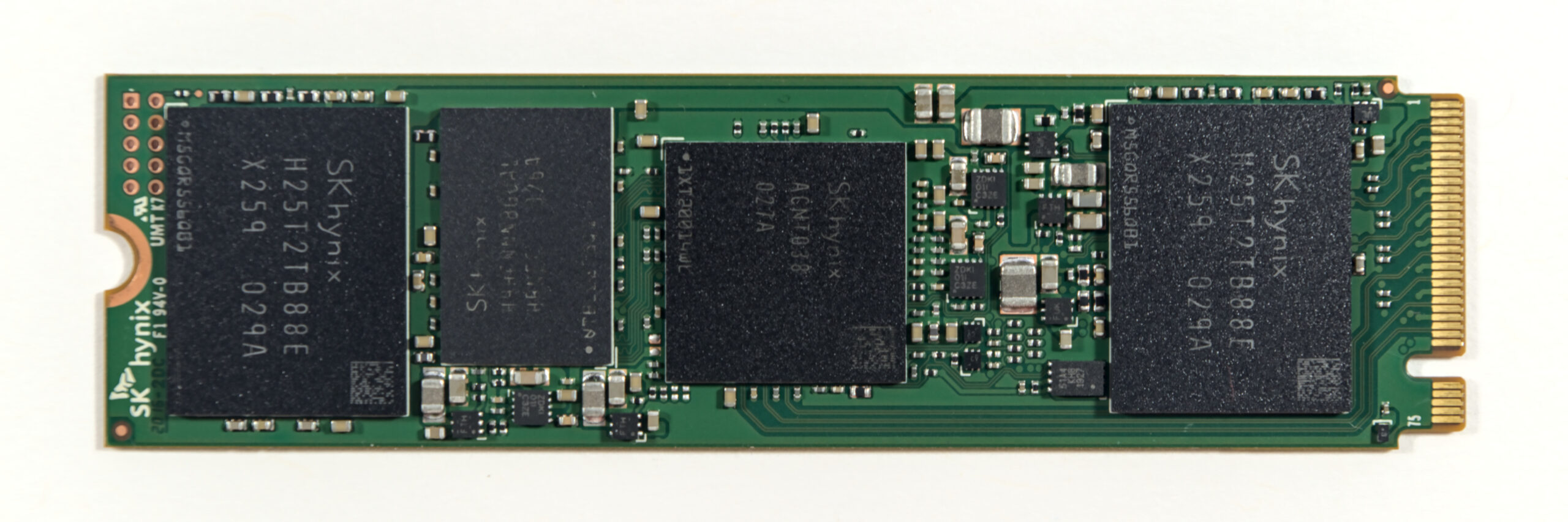
As it can be seen above, this is an all-SK hynix SSD, including the controller, RAM and flash. Using 4-channel controllers reduces the complexity of the design, as fewer traces are needed between the NAND and the controller. The controller and is packaging can also be simpler and smaller, as it can do away with fewer faster NAND channels.
In 2022, we’ve had 232-layer 3D NAND from YMTC49 (Yangtze Memory Technologies Co.) running at 2400MT/s, packing 1024Gb or 128GB per die, while other manufacturers mostly had 176-layer products being mass produced at the time50. The problem is, of course, that being Chinese-made, these flash chips are not particularly popular with the western name brand manufacturers, so they are mostly used in Chinese drives, from the likes of Zhitai and Fanxiang.
Leave a Reply